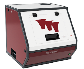
• 149mm x 149mm maximum writing area.
• 155mm x 155mm x 7mm maximum wafer size.
• 1µm minimum feature size across full writing area.
• 405nm long-life semiconductor lightsource suitable for broadband, g- and h-line positive and negative photoresists (e.g. S1800, ECI-3000, MiR 701). Replacement 385nm and 365nm lightsources available as option, suitable for g-, h- and i-line photoresists (e.g. SU-8).
Dual wavelength option (405nm lightsource and 365nm lightsource, software selectable) available for best performance across g-, h-, and i-line photoresists.
• XY interferometer with 15nm resolution for precise motion control.
• Fast writing speed: up to 50mm2/minute (1µm minimum feature size), allowing a typical 50mm x 50mm area to be exposed in under 1 hour.
• Autofocus system using yellow light with real-time surface tracking laser– no minimum wafer size.
• High quality optical microscope with Olympus infinite conjugate x10 plan objective lens and yellow light illumination for alignment to lithographic markers on the wafer (±2µm 3σ alignment accuracy). Additional x4 digital zoom can be selected in software.
• Grey scale exposure mode for 3-dimensional patterning (255 grey levels).
• Software API for external interfacing and control.
• 100nm minimum addressable grid; 15nm sample stage resolution.
• Acceptable file formats: CIF, GDS2, BMP, TIFF, JPEG, PNG, GIF. Oasis, DXF, Gerber RS-274X acceptable via KLayout conversion.
• Autocalibration tool allowing users to check and correct calibration.
• 2D barcodes can be automatically generated through software for exposures. The software can then identify the developed barcode patterns and reads the contents.
• External dimensions: 700mm (w) x 700mm (d) x 750mm (h), excluding computer.
• Light-excluding enclosure with safety interlock.
• Designed for desktop use – no optical table required.
• Easy to use, Windows® based control software supplied.
• Supplied with KLayout open-source mask design software (www.klayout.de)
• Supplied with pre-configured 64-bit Windows® 10/11 PC and monitor for ‘plug and play’ installation.
• All cables supplied.
• Extremely competitively priced for University and industrial R&D budgets.
• Can be later upgraded to MicroWriter ML®3 Baby Plus, Mesa or Pro for higher performance.
• CE-marked and compliant with EN-61010.
• 90-260 VAC, 50-60Hz, 4A single phase power requirement.

• 149mm x 149mm maximum writing area.
• 155mm x 155mm x 7mm maximum wafer size.
• 1µm and 5µm minimum feature sizes across full writing area.
• Automatic selection of resolution via software – no manual changing of lens required.
• 405nm long-life semiconductor lightsource suitable for broadband, g- and h-line positive and negative photoresists (e.g. S1800, ECI-3000, MiR 701). Replacement 385nm and 365nm lightsources available as option, suitable for g-, h- and i-line photoresists (e.g. SU-8).
Dual wavelength option (405nm lightsource and 365nm lightsource, software selectable) available for best performance across g-, h-, and i-line photoresists.
• XY interferometer with 15nm resolution for precise motion control.
• Fast writing speed: up to 50mm2/minute (1µm minimum feature size) and 180mm2/minute (5µm minimum feature size), allowing a typical 50mm x 50mm area combining critical and non-critical areas to be exposed in under 30 minutes.
• Autofocus system using yellow light with real-time surface tracking laser– no minimum wafer size.
• High quality infinite conjugate optical microscope camera with x3 aspheric objective lens and x10 Olympus plan objective lens and yellow light illumination for alignment to lithographic markers on the wafer (±1µm 3σ alignment accuracy).
• Automatic changing between microscope magnifications via software – no manual changing of lens required. Additional x4 digital zoom can be selected in software.
• Grey scale exposure mode for 3-dimensional patterning (255 grey levels).
• Software API for external interfacing and control.
• 60nm minimum addressable grid; 15nm sample stage resolution.
• Acceptable file formats: CIF, GDS2, BMP, TIFF, JPEG, PNG, GIF; Oasis, DXF, Gerber RS-274X acceptable via KLayout conversion.
• Automatic laser-based wafer centring tool.
• Built-in 2-dimensional optical surface profiler (200nm thickness resolution) for examining exposed resists, deposited layers, etching and other MEMS process steps.
• Automatic wafer inspection tool allowing each die on a wafer to be imaged.
• Autocalibration tool allowing users to check and correct calibration.
• 2D barcodes can be automatically generated through software for exposures. The software can then identify the developed barcode patterns and reads the contents.
• External dimensions: 700mm (w) x 700mm (d) x 750mm (h), excluding computer.
• Light-excluding enclosure with safety interlock.
• Designed for desktop use – no optical table required.
• Easy to use, Windows® based control software supplied.
• Supplied with KLayout open-source mask design software (www.klayout.de)
• Supplied with pre-configured 64-bit Windows® 10/11 PC and monitor for ‘plug and play’ installation.
• All cables supplied.
• Extremely competitively priced for University and industrial R&D budgets.
• Can be later upgraded to MicroWriter ML®3 Mesa or Pro for higher performance.
• CE-marked and compliant with EN-61010.
• 90-260 VAC, 50-60Hz, 4A single phase power requirement.

• 149mm x 149mm maximum writing area.
• 155mm x 155mm x 7mm maximum wafer size.
• 0.6µm, 1µm and 5µm minimum feature sizes across full writing area.
• Automatic selection of resolution via software – no manual changing of lens required.
• 405nm long-life semiconductor lightsource suitable for broadband, g- and h-line positive and negative photoresists (e.g. S1800, ECI-3000, MiR 701). Replacement 385nm and 365nm lightsources available as option, suitable for g-, h- and i-line photoresists (e.g. SU-8).
Dual wavelength option (405nm lightsource and 365nm lightsource, software selectable) available for best performance across g-, h-, and i-line photoresists.
• XY interferometer with 15nm resolution for precise motion control.
• Fast writing speed: up to 15mm2/minute (0.6µm minimum feature size), 50mm2/minute (1µm minimum feature size) and 180mm2/minute (5µm minimum feature size), allowing a typical 50mm x 50mm area combining critical and non-critical areas to be exposed in under 30 minutes.
• Autofocus system using yellow light with real-time surface tracking laser– no minimum wafer size.
• High quality infinite conjugate optical microscope with x3 aspheric objective lens, x10 Olympus plan objective lens, and x20 Olympus plan apochromat objective lens, and yellow light illumination for alignment to lithographic markers on the wafer (±1µm 3σ alignment accuracy).
• Automatic changing between microscope magnifications via software – no manual changing of lens required. Additional x4 digital zoom can be selected in software.
• Grey scale exposure mode for 3-dimensional patterning (255 grey levels).
• Software API for external interfacing and control.
• 30nm minimum addressable grid; 15nm sample stage resolution.
• Acceptable file formats: CIF, GDS2, BMP, TIFF, JPEG, PNG, GIF; Oasis, DXF, Gerber RS-274X acceptable via KLayout conversion.
• Automatic laser-based wafer centring tool.
• Built-in 2-dimensional optical surface profiler (200nm thickness resolution) for examining exposed resists, deposited layers, etching and other MEMS process steps.
• Automatic wafer inspection tool allowing each die on a wafer to be imaged.
• Autocalibration tool allowing users to check and correct calibration.
• 2D barcodes can be automatically generated through software for exposures. The software can then identify the developed barcode patterns and reads the contents.
• External dimensions: 700mm (w) x 700mm (d) x 750m (h), excluding computer.
• Light-excluding enclosure with safety interlock.
• Designed for desktop use – no optical table required.
• Easy to use, Windows® based control software supplied.
• Supplied with KLayout open-source mask design software (www.klayout.de)
• Supplied with pre-configured 64-bit Windows® 10/11 PC and monitor for ‘plug and play’ installation.
• All cables supplied.
• Extremely competitively priced for University and industrial R&D budgets.
• Can be later upgraded to MicroWriter ML®3 Pro for higher performance.
• CE-marked and compliant with EN-61010.
• 90-260 VAC, 50-60Hz, 4A single phase power requirement.
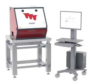
• 195mm x 195mm maximum writing area.
295mm x 295mm maximum writing area available as an option.
• 230mm x 230mm x 15mm maximum wafer size.
330mm x 330mm x 15mm (customisable up to 330mm x 330mm x 175mm) maximum wafer size available as an option.
• 0.6µm, 1µm, 2µm and 5µm minimum feature sizes across full writing area. 0.4um minimum feature size available as an option.
• Automatic selection of minimum feature size via software – no manual changing of lens required.
• 385nm long-life semiconductor light source, suitable for broadband, g-, h- and i-line positive and negative photoresists (e.g. S1800, ECI-3000, MiR 701, SU-8). Replacement 365nm lightsource available as option for improved performance with SU-8 photoresist. Dual wavelength option (405nm lightsource and 365nm lightsource, software selectable) available for best performance across g-, h-, and i-line photoresists.
• XY interferometer with 1nm resolution for precise motion control.
• Extremely fast writing speed – up to: 15mm2/minute (0.6µm minimum feature size), 50mm2/minute (1µm minimum feature size), 120mm2/minute (2µm minimum feature size) and 180mm2/minute (5µm minimum feature size). These allow a typical 50mm x 50mm area combining critical and non-critical areas to be exposed in under 30 minutes or a typical 100mm x 100mm area to be exposed at 2µm minimum feature size in under 2 hours.
• Autofocus system using yellow light with real-time surface tracking laser– no minimum wafer size.
• High quality infinite conjugate optical microscope with x3 aspheric objective lens, x5 and x10 Olympus plan achromatic objective lens, x20 Olympus plan apochromat objective lens, and yellow light illumination for alignment to lithographic markers on the wafer (±0.5µm 3σ alignment accuracy). x50 Olympus plan apochromatic objective lens available as an option.
• Automatic changing between microscope magnifications via software – no manual changing of lens required. Additional x4 digital zoom can be selected in software.
• Grey scale exposure mode for 3-dimensional patterning (up to 768 grey levels).
• Software API for external interfacing and control.
• 30nm minimum addressable grid. 12.5nm minimum addressable grid available as an option. 4nm sample stage resolution.
• Acceptable file formats: CIF, GDS2, BMP, TIFF, JPEG, PNG, GIF; Oasis, DXF, Gerber RS-274X acceptable via Clewin 6 conversion.
• Automatic laser-based wafer centring tool.
• Built-in 2-dimensional optical surface profiler (100nm thickness resolution) for examining exposed resists, deposited layers, etching and other MEMS process steps.
• Automatic wafer inspection tool allowing each die on a wafer to be imaged.
• Virtual mask aligner mode in which the pattern to be exposed is displayed on top of the real-time microscope image, allowing the machine to be used like a traditional mask aligner.
• Autocalibration tool allowing users to check and correct calibration.
• 2D barcodes can be automatically generated through software for exposures. The software can then identify the developed barcode patterns and reads the contents.
• Emailing multiple users when exposures are finished.
• Multiple wafer / chip handling, allowing different exposure patterns and alignment coordinates to be supplied for multiple wafers or chips on the chuck. Used for exposing multiple users’ samples overnight.
• Includes passive vibration-isolation optical table.
• Light-excluding enclosure with safety interlock and temperature compensation to ±0.25⁰C
• Easy to use, Windows® based control software supplied.
• Supplied with Clewin 6 mask design software.
• Supplied with pre-configured 64-bit Windows® 10/11 PC with monitor, keyboard and mouse.
• Includes on-site installation by trained service technician.
• Extremely competitively priced for University and industrial R&D budgets.
• 90-260 VAC, 50-60Hz, 4A single phase power requirement.
• Footprint 90cm (w) x 75cm (d); height 153cm (including optical table; excluding PC workstation).
• CE-marked and compliant with EN-61010.
